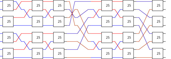
![]()
Satnam Singh
![]()
1 October 2009.
Lava is an experimental
system design to aid the digital design of circuits by providing a powerful
library for composing structural circuit descriptions. Lava is designed
to help specify the layout of circuits which can improve performance and
reduce area utilization. An implementation of Lava for Xilinx's FPGAs
can be found at Hackage and installed with "cabal install xilinx-lava".
The
following pages give a flavor of the Lava HDL and how it can be
used to describe circuits for implementation of Xilinx's Virtex
family of FPGAs. These pages assume a good understanding of Xilinx's
Virtex FPGA architecture and of the Haskell lazy functional
programming language. The number of people that know about both can easily fit
inside a medium sized elevator. So it may be useful to read A
Gentle Introduction to Haskell if you are unfamiliar with functional
programming languages. Information about Xilinx's FPGA can be
found at http://www.xilinx.com. A detailed
set of Lava tutorials are also available. Structural
netlists are described in Lava by composing functions that represent
basic library elements or composite circuits. This is very similar
to the way the structural netlists are described in VHDL or in Verilog
which rely on netlist naming to compose circuit elements. Later
we present combinators which provide a much more powerful way to
combine circuits. Most
hardware description languages provide a library of basic gates
that correspond to the Xilinx Unified Library components. Designers
can build up netlists by creating instances of these abstract gates
and writing them together. The implementation software maps these
gates to specific resources on the FPGA. Most logic functionality
is mapped into the slices of CLBs. The
top half of a Virtex-II slice is shown below: Lava
provides a more direct way to specify the mapping into CLB, slices
and LUTs. Just like the Xilinx Unified Library the Xilinx Lava library
contains specific functions (circuits) that correspond to resources
in a Virtex slice e.g. muxcy and xorcy. However, instead of trying
to enumerate every possible one, two, three and four input function
that can be realized in a LUT Lava instead provides a higher order
function for creating a LUT configuration from a higher level specification
of the requited function. As
an example consider the task of configuring a LUT to be a two input
AND gate. This can be performed by using the lut2
combinator with an argument that is the Haskell function that performs
logical conjunction written as &. The
lut2 higher order combinator takes any function
of two Boolean parameters and returns a circuit that corresponds
to a LUT programmed to perform that function. A circuit in Lava
has a type that operates over structures of the Bit type. The and2
circuit is defined to take a pair of bits as input and return a
single bit as its output. Note
that lut2 is a higher order combinator
because it takes a function as an argument (the &
function) and returns a function as a result (the circuit which
ANDs its two inputs). Indeed the lut2 combinator
can take any function that has the type Bool
-> Bool -> Bool and it returns
a circuit of type (Bit, Bit) -> Bit.
The type of the lut2 function is similar to: When
Lava generates a VHDL or EDIF netlist for this component it will
instance a LUT with the appropriate programming information. Here
is what the generated VHDL for the and2
gate might look like: When
realized in the top part of a slice as shown in the picture above
this gate would be mapped to the upper G function generator which
will be configured as a LUT. As
another example consider the definition of a three input AND-gate.
First, we define a function in Haskell that performs the AND3 operation: The
first line gives the type of and function as something that takes
three boolean values and returns a boolean value. The next line
defines the and3function in terms of the
Haksell binary & function. Now we
are in a position to define a circuit that ANDs three inputs: The
general idea is that instead of trying to provide a library that
tries to enumerate some of the one, two, three and four input logic
functions Lava provides four combinators lut1,
lut2, lut3 and lut4.
These combinators take functions expressed in the embedding language
(Haskell) and return LUTs that realize these functions. This makes
it convenient to express exactly what gets packed into one LUT.
Later we will see that these higher order combinators are actually
overloaded which allows LUT contents to be specified in many different
kinds of ways (including an integer or a bit-vector). Lava
does provide a module that contains definitions for commonly used
gates mapped into LUTs. These include: assuming
the following functions are available in addition to the Haskell
prelude: To
make a netlist that corresponds to a NAND gate one could simply
perform direct instantiation and wire up the signals appropriate
just like in VHDL or Verilog: Lava
generates a netlist containing two LUT instantiations for this circuit:
a LUT2 to implement the AND gate and a LUT1 to implement the inverter.
How many LUTs are used to realize this circuit on the FPGA? If no
information is given about the location of these two circuits then
the mapper is free to merge both the LUT2 for the AND gate and the
LUT1 for the inverter into one LUT. However, if the inverter has
been laid out in a different location from the AND gate then the
two components will not be merged. By default each gate is at logical
position (0.0). Since the description above does not translate the
two sub-circuits to another location they are understood to occupy
the same function generator location and will be merged into one
LUT. A
partial list of some of the basic Virtex slice resources supported
by Lava is shown below:
Lava uses a Cartesian coordinate system with the origin at the bottom
left hand corner of the screen. A Lava design can have many independent
coordinate systems and each of these will be represented by an H_SET
in the implementation netlist. The Lava coordinate system is designed
to make it easier to produce circuit descriptions that are portable
between the Virtex and Virtex-II architectures by abstracting as
much as possible the CLB and slice boundaries. Circuits
are conceptually enclosed in rectangular tiles which can be laid
out relative to each other. There are two kinds of tiles that Lava
supports: (a) two-sided tiles which communicate only along their
left and right hand sides and (b) four sided tiles that can communicate
along all four sides of the tile.
The serial composition combinator in Lava is written as >->
and it takes two circuits as its arguments and returns a new composite
circuit. This combinator performs two distinct functions:
An example of serial
composition is shown below for the circuit and2
>-> inv. The circuit and2 takes
a pair of signals as its input and returns a single output bit.
This is illustrated in the diagram below: The
and2
circuit is realized in a two-sided Lava tile which means that signals
(either inputs or outputs) can occur on the left or right hand sides
of the tile but not the top or bottom. The inv
circuit is also realized in a two-sided tile. To make an NAND gate
form these components all one needs to do is to connect the output
of one circuit to the input of the other circuit. This task can
be performed by the serial
composition combinator without having to name the intermediate
signals. However
the serial composition combinator does more than just connect wires
together. Serial composition looks at the sizes of the circuits
it has to compose and it lays out one circuit directly next to the
other circuit with their bottoms aligned. For example consider the
tiles containing the inv and and2
gates which which each have size (1,1). The serial composition combinator
takes the output of the and2 gate and
connects it to the input of the inv gate
resulting in a circuit that behaves like a NAND-gate. It also places
the inv gate to the right of the and2
gate so it ends up in location (1,0). The composite NAND-gate circuit
tile has size (2,1) as shown below. When
Lava generates an EDIF netlist it translates its own coordinate
system into an appropriate coordinate system for the chosen target
architecture. For Virtex family devices it will generate relative
location attributes using CLB and slice coordinates. The and2
gate at Lava location (0,0) will be mapped to R0C0.S1 (the left
hand slice of a CLB at relative location (0,0)). The inv
gate will be mapped from the Lava location (1,0) to R0C0.S0 (the
right hand slice of a CLB at relative location (0,0)). The absolute
location of the circuit on the FPGA is left to the Xilinx placer.
The corresponding layout on a Virtex XCV300 FPGA is shown below
(captured from the Xilinx FPGA Floorplanner): The
and2 gate at Lava location (0,0) has been
mapped into the upper LUT of the left hand slice of the CLB at R32C1
i.e. R32C1.S1 (the left hand corner of this Virtex device). The
inv component has been mapped into the
upper LUT of the right hand slice in the same CLB i.e. R32C1.S0.
Note that within the slice the Xilinx tools are free to map to either
the upper or lower LUT (F or G). Lava coordinates can specify which
logic should be mapped into a slice by requesting either F (y coordinate
an even number) or G (y coordinate an odd number) in a relative
coordinate system but the Xilinx mapper will decide the actual mapping
and absolute location. For
the Virtex-II architecture Lava generates slice-based coordinates. Parallel Composition
The
serial composition combinator is useful when we wish to compose
and lay out two circuits that communicate. Sometimes however we
wish to lay out circuits relative to each other which do not communication.
One of the many combinators that Lava provides for composing circuits
in parallel
is the par2 combinator. This combinator
takes two two sided tiles and placed the second tile above the first
tile aligned along their left hand edges. An example layout for
the circuit par2
inv and2 is shown below: Any
circuit or combinator that takes two inputs can be written as in
infix operator in Lava by enclosing the name of the circuit or combinator
in back quotes as shown above i.e. par2
inv and2 is the same as inv `par2`
and2. The par2 combinator
produces a composite circuit that takes a two element tuple as its
input and returns a two element tuple. The first element of the
input tuple is the input destined for the first (lower) circuit
and the second element of the input tuple is the input destined
for the second (upper) circuit. The first element of the output
tuple is the output from the first (lower) circuit and the second
element of the output tuple is the output from the second (upper)
circuit. The layout of the composite circuit tile of size (1,2)
in the Lava coordinate system is shown below.
The
par2 combinator operates over
just two circuits. Three or more circuits can be composed by using
par2 as an infix operator but this results in
circuits with awkward tuple types. The par combinator
takes a list of circuits (all of the same type) and lays them out
from the bottom to the top: Sometimes
it is useful to apply the same circuit to every element of an input
bus. We can use the Haskell higher order map function and the Lava
par combinator to define a circuit combinator
which performs exactly this task. The Lava combinator that maps
a circuit across a bus is called maP (with a
capital P to it does not clash with the Haskell function map) and
is defined as: This
combinator takes any circuit r (which is considered to be a two
sided tile) and replicates it as many times as there are elements
in the input bus and then layouts out these replicated circuits
vertically. For example to invert every bit on a bus one would write
maP inv
resulting in the layout shown below: Another
use of maP is to vertically place registers across each element
of a bus. The basic register in Lava that corresponds to FD takes
two inputs: the clock and the D input signal. The circuit vreg registers
each element of a bus and is define as: A
register fits in a tile of size (1,1). To describe an AND gate with
a register at the output we could use serial composition: and2Reg clk = and2 >->
fd clk This produces the following layout: Why is the register realized in the adjacent slice
and not the slice containing the function generator for the AND2
gate? This is because the and2 circuit occupies a tile of size (1,1)
and the register also occupies a tile of size (1,1) and when the
serial composition combinator is asked to put one tile next to the
other that is exactly what it does. This results in the register
being realized in location (1,0). If this is not what is wanted
then a variant of the serial composition combinator can be used
to compose two circuits without translating the second circuit.
This combinator is called the serial overlay combinator and
is written as >|>. The circuit and2
>|> fd clk will realize both the and2 circuit
and the inv circuit into location (0,0) giving: Now
the and2 gate and the FD register are
realized in the top half of one slice. Lava will always map and
place circuits exactly in the way specified by the layout combinators. The >-> serial composition
combinator only composes circuits with a left to right data-flow.
There are three other serial compositions combinators that describe
right to left (<-<), bottom to top
(/\) and top to bottom (\/)
serial composition. They are illustrated below: Beside and Below
To
describe circuits that communicate on more than two faces of a tile
Lava also provides support for four sided tiles. A circuit can be
put inside a four sided tile if it has a type which takes a two
element tuple as its input and returns a two element tuple as shown
below: A
four sided tile is divided into the input signal and output signal
portions by the gray diagonal line. The input to a circuit that
fits into a four sided tile must be a tuple (a, b) where the a signal
is connected to the bottom of the tile and the b signal is connected
to the left of the tile. These signals can be single bits or composite
signals. The result type of a circuit that fits into a four sided
tile must also be a tuple (c, d) where the c signal is connected
to the right hand side of the tile and the d signal is connected
to the top of the tile. To
put one four sided tile below another four sided tile requires a
new combinator because these tiles do not have the appropriate types
for the par2 combinator. Lava provides the below
combinator for this task and the picture below shows the circuit
r `below` s: The
circuit r has the type (e,b) -> (c, x) and the circuit s has
the type (x,e) -> (f, g) and the composite circuit has the type
(e, (b, e)) -> ((c, f), g) where x is the type of the intermediate
signal that r and s communicate along. There is also a beside
combinator that lays out s to the right of r. Row and Col Four
sided tiles can be replicated and composed to form columns and rows.
The col combinator tiles a circuit r
vertically and forms connections between the top and bottom faces
of the tile: The
row combinator composes tiles horizontally from left to right and
is based on the beside combinator. Rows and
column combinators can be used to describe many interesting layout
patterns and emulate layout grids which are not four sided. Here
is how a hex-connected grid might be described in terms of four
sided tiles: This
section describes how to design a ripple-carry adder in Lava that
uses the Virtex carry chain. This component is widely used in many
other Lava examples. First we present how to describe a one-bit
adder cell using the regular netlist style. Then we use layout combinators
to create a vertical column of these cells that make up a carry-chain
ripple-carry adder. A One-Bit
Adder A
one-bit adder can be accommodated in one half of a slice using just
one function generator as a LUT, one MUXCY and one XORCY. For this
reason we will describe the one-bit adder in netlist style. A schematic
for a one-bit carry chain adder is shown below. A
column layout combinator will be used later to tile several one-bit
adders vertically to make an n-bit adder. Before we tile
the one-bit adder vertically we have to carefully consider which
sides of the tile the signals are connected to. We shall assume
a left to right data flow with the two bits to be added connected
to the left hand side of the tile and the sum bit appearing from
the right hand side of the tile. Since the carry must flow upwards
in the Virtex architecture the cin signal must come into the bottom
of the tile and the cout signal must emerge from the top of the
tile. This gives the following four-sided tile orientation: This
four-sided tile represents a circuit with input ((a,b), cin) because
(a,b) is the left input and cin in the bottom input. This tile also
has the output (sum, cout) because sum is the right output and cout
is the top output. This fixes the type for this one-bit adder adder
tile which can now be described as a Lava netlist as follows: This
is very similar to what one would write in VHDL or Verilog except
that the instance names are anonymous. Furthermore, the Lava description
includes information in the shape of the types that indicates which
faces of the tile signals occur and in what order. This is essential
in order to compose tiles using combinators which automatically
glue together circuit interfaces and layout out circuits in specific
patterns. A 4-bit
Carry Chain Adder To
make a 4-bit adder all we need to do is to tile vertically four
one-bit adder tiles: In
a conventional HDL this can be described either by copying and pasting
the instantiating code for each one-bit adder and then naming intermediate
nets which cause components to be connected together to form the
composite four-bit adder netlist. Constructs like for...generate
in VHDL help to capture such repetition more concisely but internal
nets still have to be named and there is no information about layout.
The Lava description of the circuit show above is simply: This
is much more concise than equivalent conventional HDL descriptions.
It also includes information about layout: the first one-bit adder
tile is at the bottom and then the other are stacked on top of it
in sequence (RLOCs are generated to enforce this layout). Internal
nets are anonymous and circuits are composed automatically by taking
the input from below and attaching it to the carry input of the
tile. An
example Virtex layout of a 8-bit adder generated by the expression
col 8 oneBitAdder
is show below: In Lava a parameterized n-bit adder can be defined
as: This parameterized adder function uses an integer
parameter n to determine the size of the adder. This controls how
many one-bit adders are placed in a column. Each one-bit adder is
expecting a par of bits on its left edge. To form the correct input
for a column of one-bit adders we have to pair-wise associate the
two inputs vectors a and b. This is accomplished by using the list
processing function zip which has the
Haskell type [a] -> [b] -> [(a, b)].
For example: The use of zip in adder
ensures that the nth bit of a is
added to the nth bit of b. A specialized version of the adder which has no carry
in or carry out can defined as: This definition uses the gnd component to provide
the carry in signal and just discards the carry out. A registered 4-bit adder can be made by composing
the adderNoCarry component and the vreg component using >|>
(the serial overlay operator) to make sure the adder and register
share the same location: A parameterized n-bit registered adder can
be defined as: The Virtex layout produced for registeredAdder 4 is
shown below. This section describes how to build an adder tree
using the carry chain adders presented in the previous section. Consider the task of adding eight numbers n1, n2,
.. n8 use a binary tree of adders as shown below. In a language like VHDL one can write
a recursive function that takes an unconstrained array of numbers
as input and returns their sum computed with an adder tree. However,
there is no standard way in VHDL of specifying how the adder tree
should be laid out. Adder trees are typically pipelined and it takes
just one adder to be badly placed to degrade the performance of
the whole adder tree. Since Lava can specify how the adders are
to be laid out the design engineer can make decisions and calculations
about intermediate wire delays. One example layout scheme for a
pipelined adder tree is shown below (the clock wires are now shown): This layout scheme places the adders
in a row with the final addition occurring in the middle. Both the
left and right hand sides of the final adder also contain adder
trees in which the final sum occurs in the middle. This recursive
structure continues until the leaf additions are encountered (e.g.
the adder for n1 and n2). To help describe the idea of three components laid
out horizontally with the middle component receiving its inputs
from its neighbors we introduce the middle combinator middle
r s t which gives the following layout: Note that this combinator produces a two-sided tile
which has two inputs on the left and one output on the right. Using the middle combinator we can define a tree circuit
combinator for any kind of two input and one output circuit: A combinational adder tree with bit-growth can be made with the
flexibleAdder circuit. This circuit has
the type (Bit, Bit) -> (Bit) so it is suitable for use as an
element of an adder tree. To define a combinational adder tree one
simply writes: adderTree = tree
flexibleAdder It is possible to rewrite a call to the tree combinator
to see how it works for a particular circuit and input list: We can use the flexibleAdderFD
circuit to make a pipelined adder tree: adderTreeFD clk = tree
(flexibleAdderFD clk) The adders in this tree will use FD register components. An example
layout of four 96-input pipelined adder trees stacked upon each
other is shown below on a XCV300 part. The bit-growth in the adder
tree helps to identify the recursive nature of the layout. The adder trees shown above sum 96 9-bit numbers each
and with this layout the circuit operates at 173MHz on a XCV300
at speed grade 6. If the layout information is removed and the same
netlist is placed and routed again the maximum speed is 129MHz i.e.
34% slower. The graph below shows that specifying layout had significant
performance advantages. The blue bars represent the speed of circuits
with layout information and the red bars represented the speed of
the same netlist with the layout information (RLOCs) removed. Each
pair of bars corresponds to a target timing specification. The leftmost
pair of bars is for the case where the place and route tools were
asked to meet a timing specification of 180MHz but delivered 173MHz
for the RLOC-ed circuit and 129MHz without the RLOCs. Providing layout information also speeds out the place
and route times as shown in the graph below. For the 180MHz timespec
case the netlist with layout took less then 400 seconds to route
(nothing needs to be placed) but took more than 1800 seconds to
place and route without layout information. The FPGA Editor view of the four placed
adder trees is shown below. Without the RLOCs the following implementation is
produced: The adder tree layout was easy to express in Lava
and has produced significant performance advantages. Many other
tree layout schemes can be easily explored in Lava. It is also very
easy to make trees of other kinds of circuits like multiplier etc.
All one has to do is to supply such circuits to the first argument
of the tree combinator. This section describes how to build a constant coefficient
multiplier (KCM) for the Virtex family of FPGAs using a combination
of table lookups and additions. There are many other kinds of KCM:
this one has been chosen to help illustrate how to design with distributed
memory components in Lava. The architecture of this multiplier is based on performing
many 4-bit (or smaller) multiplications and then combining the results
of these partial products with a weighted adder tree. Optionally
the adder tree can be pipelined. The reason for performing 4-bit
multiplications is that these can be performed quickly with lookup
tables (since each LUT has four inputs). A specific multiplier generated
by the Lava KCM core is shown below. This KCM multiplies a 11-bit signed dynamic input
A = a10
..0 by a 11-bit
constant coefficient K. The multiplication
AK is performed by composing the results
of several four-bit multiplications by exploiting the identity: AK
= -28
a10 ..8 K + 24
a7 ..4 K + a3
..0 K The rightmost table multiplies the lower four bits
of the inputs by the constant coefficient i.e. X
= a3 ..0
K and the middle table computes Y
= a7 ..4
K where both a3
..0 and a7
..4
are treated as unsigned numbers. The leftmost table calculates Z
= (a10,
a10, a9,
a8)
K where (a10,
a10,
a9,
a8)
is treated as a sign-extended bit-vector. To calculate the final
results the partial products Y and Z
have to be appropriately weighted before addition A weighted adder
tree is used to compose the partial products and the size of the
intermediate adders is reduce by reading off directly the bottom
four bits of the partial product X and
the result of adding the remaining bits of X
to Y. For the pipelined version of this
multiplier Lava places registers on the intermediate wires making
sure to balance the delays. The four-bit multiplications are performed by table
lookups using distributed memory (i.e. LUTs). In this case an 11
bit constant must be multiplied by a four bit dynamic input which
requires a table with a 15-bit output. This can be easily made by
using 15 four-input LUTs all with the same input. To avoid unwanted
mapper optimizations we use the ROM16X1 component to create a LUT
with specific lookup table contents. Lava provides a family of functions that make it easy
to create tables made out of ROM16X1 components. One of the functions
available from the Lava LUTROM module is rom16x which will create
a four-input n-output table from data specified as a list of numbers. lut16x :: [Int] -> (Bit, Bit, Bit, Bit) ->
Bit The code for a four-bit unsigned KCM in Lava is shown
below. The first parameter to this function is coeif which
is the constant coefficient. The second argument is a bit-vector
which is represented as a list in Lava (with the LSB as the first
element). To allow multiplications by bit-vectors less then four
bits in width this function pads out the table with zero values
for smaller multiplications. This is done by first forming a table
of the multiplication results i.e. [coeif * i | i <- [0..2^nr_addrs-1]] which for an address less than four bits will have
less than 16 elements. Then the pad_width
function is used to add zero elements to end of the list to bring
the length of the list up to 16. The result is bound to the variable
name multiplication_results which is examined
to find the largest product which in turn is used to determine how
many output bits are required (maxwidth).
Now the product can be computed by by forming a 16 element table
with maxwidth output bits using the rom16x
function. A singed four-bit KCM can be built in a similar manner
(this time using sign extension on the input bits). To make an unsigned KCM the following steps are taken: Each of the stages described above is composed in series as shown
below for the case of a 12-bit dynamic input: Since each unsignedFourBitKCM is long and thin it
is better to lay them out horizontally by using the horizontal version
of the maP combinator called hmaP: This picture leads to the Lava definition of unsignedKCM
shown below: Note how the specific four-bit KCM circuit to be used
is passed as a higher order parameter. The unsignedKCM
higher order circuit can be instantiated with a specific four-bit
KCM to make either combinational or sequential KCMs. Similarly the
adderTree circuit is passed as a higher
order circuit. To make a specific unsigned KCM we also need to specify
exactly which adder tree circuit to use. If we used a combinational
weighted tree the resulting KCM would be a combinational circuit.
To help design a weighted adder we define a type that describes
the "virtual" signals that flow along the wires of a weighted
adder. The type WtNr is defined to be
a tuple which contains a weight represented as an integer and a
bit-vector. These signals are called "virtual" because
the weight component is an integer which is only used during elaboration
and does not correspond to a wire in the circuit. type WtNr = (Int,
[Bit]) The unsignedWeightedAdder
circuit takes a pair of such weighted numbers and returns a weighted
number. This is expressed by the following type signature: This circuit assumes the first element of the input
pair has a larger weight than the second element. If this is not
the case this circuit calls itself again with the elements of the
pairs swapped. This is achieved by using a pattern match guard to
ensure that the first input has a higher weight than the second
input: Otherwise unsignedWeightedAdder
computes the difference between the two weights to compute how many
of the lower bits of the second input to pass through. The remaining
bits are then added to the first input to compute the upper bits
of the final sum. The weight of the result is the higher input weight
and the resulting addition is formed by composing the bit-vector
from the addition with the lower bits. Putting these lines of code together produces the
complete code for the unsignedWeightedAdder circuit: To make a specific unsigned combinational KCM we just
need to give a tree of unsigned weighted adders to the unsignedKCM
circuit: To make a pipelined KCM we need to provide the unsignedKCM
circuit with a pipelined version of the four-bit KCM circuit and
a pipelined version of the weighted adder tree circuit. A pipelined
version of the four-bit KCM just places a register at the output
of the lookup tables with a C clock input and a CE clock enable
input. This circuit is called unsignedFourBitKCMCE
and is easily defined as: i.e. a combinational four-bit unsigned KCM serially
composed (by overlaying) with a register-bus with clock and clock
enable inputs. An unsigned weighted adder tree can be made by making
a tree of unsigned weighted adders that have their outputs registered
in a similar manner. This allows a registered unsigned KCM to be
defined as: Note how much of the commonality of the basic structure
of the combinational and pipelined KCMs has been captured by the
unsignedKCM higher order circuit. The layout produced for a pipelined unsigned 11-bit
dynamic input and 11-bit constant is shown below for a Virtex part. On a XCV300-4-BG432 part this circuit runs at a speed
of at least 196MHz. The layout for an unsigned KCM with a 32-bit
dynamic input and an 11-bit coefficient is shown below. The 4-bit multiplications occur in the rectangular
block on the left and the weighted adder tree is shown on the right
hand side of the picture. On a XCV300-4-BG432 this circuit operates
at a speed of at least 130MHz. Many other layouts are possible e.g.
to place the 4-bit multiplications closer to their corresponding
adders at the leaves of the adder tree. This section describes how to build a sorter circuit
using butterfly networks which are carefully placed to ensure high
performance. The sorter circuit is made by recursively merging the
results of sub-sorts. A top-level schematic of the circuit that
we present in this section is shown below. The merger that we present
is bitonic which requires the first half of the input list to be
increasing and the second half decreasing (or vice versa). The result
of the top sorter is reversed to accommodate this requirement. Given the ability to sort two numbers and the diagram
above we have a recursive formula for making sorters of any size.
First the availability of a two sorter is assumed and the merger
is designed. Then the implementation of the two sorter is given. A merger called Batcher's Bitonic Merger can be made
by using a butterfly of two sorters. Here is an example of a specific
butterfly network of two sorters (written as 2S) which merges eight
numbers: To help describe such butterfly networks in Lava a
few useful circuit combinators are introduced. From the top level description we see that a reverse
operation is required and we can simply use the built in Haskell
reverse function: Another very useful wiring combinator is called riffle
and an instance of it is shown below: This wiring combinator interleaves the odd and even
elements of the input list (shown on the left). It can be defined
in Lava as: The halve function splits a list into two halves which
are returned in a two element tuple. The ziP combinator takes a
pair of lists and returns a new list of pairs by associating each
element in the first list with the corresponding element in the
second list. The unpair function then flattens this list of pairs
into a list. It is also useful to be able to perform the inverse
function of riffle called unriffle. This circuit can be thought
of as the reflection of the riffle circuit along a vertical axis
as shown below. The definition of unriffle in Lava is given below. Sometimes a bus containing n elements is processed
by using two copies of a circuit such that the first copy of the
circuit operates on the bottom half of the input and the second
copy of the circuit operates on the top half of the input as shown
below for a four input bus: The combinator that performs this task
is called two and is easily defined
in Lava: two r = halve >-> par
[r,r] >-> unhalve Note that this combinator placed the
first copy of r below the second copy of r. A specific instance
of this combinator is two
two_sorter which is shown below: Another combining form that uses two
copies of the same circuit is ilv
(pronounced "interleave"). This combinator has the property
that the bottom circuit processes the inputs at even positions and
the top circuit processes the inputs at the odd positions. An instance
of ilv R for an eight input bus is shown below. The ilv
combinator can be defined by noticing the it is the composition
of an unriffle, two R and riffle: The evens combinator chops the input list into pairs
and then applies copies of the same circuit to each input. The argument
circuit for evens must be a pair to pair circuit. An instance of
evens two_sorter over an eight input list is shown below. This combinator is defined as: Using the combinators shown above we can now describe
a butterfly network of some circuit r (such that r is a pair to
pair circuit): Here is a picture of bfly r 1: This makes sense in the case of a two sorter since
a butterfly of size 1 has 2 inputs which can be sorted by a single
two sorter. The layout for bfly r 2 is: The left hand side of this picture shows
an interleave of R and the right hand side shows evens R. The layout
for bfly r 3 is: Note that a sub-butterfly of size 2 has
been identified with a pale background. It can be instructive to
unfold the bfly r 3 expression and then try and spot where the various
combinators occur in the picture. To make a merger all we need to do is to instance
this butterfly with a two sorter. Here is a picture of bfly r two_sorter
(also shown before): This solves the right hand side of the sorter architecture
since bfly two_sorter makes a bitonic merger: The two remaining sorters can be recursively decomposed
using exactly the same technique used to decompose the top level
sorter. For example, the upper sorter can be implemented by using
a merger (shown on the right) and then sorting the two sub-lists.
Since each sub-list contains just two elements we get to the base
case of the recursion and deploy a two sorter. But how is the merger realized? As before, it is just
a butterfly of two sorters, in this case bfly 2 two_sorter: Applying the same technique to the lower sorter gives
the complete architecture for a size 3 sorter (i.e. 2^3 inputs =
8): Although it is not at all obvious this circuit sorts
eight numbers it has been systematically derived from a simple procedure
which can be codified in Lava as: This description says that a sorter of degree 1 (i.e.
2 inputs) can be made using a two sorter. A larger sorter is made
by using two small sorters, then reversing the result of the upper
sort, and then merging these sub-sorts using a butterfly of two
sorters. Note that this sorter description is parameterized on the
specific sorter to be used. An instance of sorter two_sorter produces a pipelined
8 input sorter which is shown below on a Virtex-II device: Note that since Lava combinators include layout as
well as connectivity information the resulting circuit occupies
a rectangular area which corresponds to the pictures shown above. A degree 4 (i.e. 16 inputs) sorter is shown below: A degree 5 (i.e. 32 inputs) sorter is shown below: A slightly larger version of the network above which
sorts 32 16-bit numbers each clock tick operates at 165MHz on a
XC2V3000 part with a latency of 14 clock ticks (using the 4.1i version
of the Xilinx design tools). Larger data-sets can be sorted by storing
numbers in BlockRAM and then iteratively sorting and merging. More
details can be found in the paper
Design
and Verification of a Sorter Core. Some instances of these butterfly networks were implemented
on a XCV300 FPGA and ChipScope was used to verify that the real
hardware actually did sort numbers: This section describes how to build a one dimensional
(1D) systolic filter in Lava. First we present the design of the
processing element of the systolic array. Then we show how this
processing element can be replicated to form a filter. Note that
there are many ways of designing such filters and this technique
is not the best possible implementation on Xilinx's FPGA architectures.
This example has been chosen to help illustrate how to describe
systolic-style systems in Lava. NOTE: The filter implementations presented
here are designed to illustrate aspects of Lava and are not the
recommended implementations for Xilinx's FPGAs. Xilinx's Core Generator
contains several optimized filter implementations. The filter we shall build is called a finite impulse
response filter (FIR) digital filter which calculate the weighted
sum of the current and past inputs. FIR filters are also known as
transversal filters or as a tapped delay line. The behavior of the
finite impulse response filter can be described by the equation: where yt
denotes the output at time t and xt
represents the input at time t
and ak
are the filter coefficients We shall use an "inner product"
processing element to perform a single multiplication and addition
and then replicate this processing element to make a circuit that
compute the filtering function. We shall assume at the coefficients
are constants which will allow us to use constant coefficient multipliers
in our implementation. We can model a finite impulse response filter in Haskell
(the host language of Lava) with the following code. This function takes three arguments: If the input stream is empty i.e. the empty list [] then this function
returns the empty list. If the input stream is non-empty then the
first value in the input list is bound to xin and the remainder
of the list is bound to xrest. The xvals are paired for multiplication
up with their corresponding weight values by using the zip list
processing function (for matching up elements pair-wise across two
lists). The products are added to yield the filter result for this
tick. This result is then followed by a list that corresponds to
the remainder of the input stream (xrest) being recursively processed
by the same function. However, we have to shift along the xvals
so the xin value appears at the first tap. The expression (init
xvals) returns the original xvals list with the last element removed.
This allows us the express the "shifting in" of the new
x value with the expression xin : init xvals. Although the semisystolicFIR function does not correspond to a
Lava circuit it can be used to simulate a filter. For example, assuming
we have an input stream which corresponds to sine wave (scaled by
127) we can calculate the result of applying a finite impulse response
filter with weights1 =[3, 9, 15, 7, 5]. Here is the results of performing
such a simulation at the prompt of the ghci Haskell interpreter
(looking at only the first 10 values of the input and output). Systolic1DFir> take 10 sineValues [0,9,18,26,35,43,52,60,67,75]
Systolic1DFir> take 10 (semisystolicFIR weights1 [0,0,0,0,0] sineValues)
[0,0,27,135,375,672,1005,1340,1668,1997] As a final step a filtering function may divide the output by the
sum of the coefficients which will scale the output signal back
into the range of the input signal (this is note done by this implementation).
Choosing coefficients that have sum which is a power of two make
it easy to perform such scaling since this corresponds to throwing
allow some of the low order bits. First we describe a semi-systolic filter. In a systolic
design all the wires between processing elements have at least one
latch and all the latches have the same clock signal. In a semi-systolic
design this constraint is relaxed to allow wires between processing
elements which do not have any latches. The inner product processing element will take as
inputs an accumulated sum from previous processing elements (yin),
a filter coefficient (ai) and a sample
value from the input stream (xin)
and return two values: the xin is
passed to xout and the yout is computed
by performing the inner product calculation and adding it to the
accumulated sum i.e. yout = yin
+ ai * xin.
An implementation for an inner product processor is shown below
where the purple circle denotes a constant coefficient multiplication
by the value ai and the green circle
denotes an adder. The input x values are passed from left to right
and the accumulated sums as passed right right to left. To make a complete filter we need a way of sequencing
the x values one at a time through each processing element. This
can be accomplished by placing a register at the xin
input of the inner product processing giving the following processing
element: A semi-systolic filter can now be made
by composing several comprises of this processing element. We need
one processing element for each tap in the filter so a four tap
filter would like look: This is a semi-systolic filter because
although there are registers on the wires carrying the x values
there are no registers on the wires that carry the accumulated sum.
The critical path of this circuit goes through four processing elements
which makes this a poor implementation choice. The Lava description of this filter can
be used to generate VHDL for simulation and EDIF for implementation
using Xilinx's place and route tools. The VHDL simulation shows
that the filter behaves as expected: The layout of this filter is shown below
implemented in the corner of a Virtex-II FPGA (an XC2V1000-FF896
with speed grade 6). This adders grow taller in a left to
right direction as the accumulated sum gets larger. This implementation
has a maximum combinational delay of 14.527ns (as reported by the
place and route tools) which gives a maximum frequency of 68.8MHz
and has 14 logic levels. This implementation uses 119 slices. This
layout can be compacted by overlapping some of the pipeline registers
with the result of the KCM calculation which also results in a faster
implementation. A better filter can be made by transforming
this semi-systolic filter into a systolic filter by the systematic
application of three techniques: retiming, slowdown and hold-up. The processing element of the 1D systolic FIR is shown
below. Both the x values and the accumulated results flow from left
to right. Registers are added at the inputs and outputs for pipelining
in a way that makes sure the accumulated sums and x values stay
in synch. This circuit can be specified by the
Lava code below which makes use of a KCM and an adder that were
presented earlier. An example of a four tap filter using this processing element is
shown below: This is formed by simply replicating the processing element horizontally.
The x input has to be delayed by one clock tick to synchronize with
the y inputs. When this filter is implemented by the Xilinx place
and route tools the last two registers on the x path are automatically
pruned as is the unused xout signal.
The Lava code for this filter is shown below. This filter has a much higher latency (8 ticks) than the semi-systolic
filter: However, since the longest combinational path between any two registers
goes through just one processing element. The place and route tools
report a maximum clock period of 6.687ns which allows this filter
to be run at 150MHz. A more compact but slower filter can be made by realizing the multiple
register stages with SRL16 components (shift registers implemented
in LUTs which can shift by up to 16 stages). A better implementation can be produced by transforming the semi-systolic
implementation into a systolic implementation by the systematic
application of three techniques: retiming, slowdown and hold-up. Although the semi-systolic filter is not recommended for FPGA implementation
we reproduce the implementation and show how it can be captured
in Lava. This architecture can not be directly described by the Lava combinators
introduced so far because there is both left to right and right
to left data-flow through each block. To help describe such communication
patterns we introduce a new combinator called two-way serial and
written as >< : This combinator can then be used to describe a combinator called
twoWayRow for the serial composition of
many identical blocks that have two-way data-flow: The definition of twoWayRow is: twoWayRow = foldl1 (><) This combinator can now be used directly to describe the semi-systolic
filter shown above. Describing Netlists in Lava

and2 :: (Bit, Bit) -> Bit
and2 = lut2 (&)
lut2 :: (Bool -> Bool -> Bool) -> ((Bit, Bit) -> Bit)
lut2_1 : lut2 generic map (init => "1000")
portmap (i0 => lava(5), i1 => lava (6),
o => lava(4)) ;
and3function :: Bool -> Bool -> Bool -> Bool
and3function a b c = a & b & c
and3 = lut3 and3function
inv = lut1 not
and2 = lut2 (&)
or2 = lut2 (||)
xor2 = lut2 exor
muxBit sel (d0, d1)= lut3 muxFn (sel, d0, d1)
exor :: Bool -> Bool -> Bool
exor a b = a /= b
muxFn :: Bool -> Bool -> Bool -> Bool
muxFn sel d0 d1
= if sel then
d1
else
d0
nandGate (a, b) = d
where
d = inv c
c = and2 (a, b)
gnd :: Bit
vcc :: Bit
fd :: Bit -> Bit -> Bit
fde :: Bit -> Bit -> Bit -> Bit
muxcy :: (Bit, (Bit, Bit)) -> Bit
muxcy_l :: (Bit, (Bit, Bit)) -> Bit
xorcy :: (Bit, Bit) -> Bit
xorcy_l :: (Bit, Bit) -> Bit
muxf5 :: (Bit, (Bit, Bit)) -> Bit
muxf6 :: (Bit, (Bit, Bit)) -> Bit
muxf7 :: (Bit, (Bit, Bit)) -> Bit
muxf8 :: (Bit, (Bit, Bit)) -> Bit
Layout in Lava
The Lava Coordinate System
Serial Composition
maP r = par (repeat r)
vreg clk = maP (fd clk)
Serial Overlay Combinator


Describing Non Left-to-Right Dataflow
Four Sided Tiles
An Adder Example
A Ripple Carry Adder Example (using the Virtex Carry Chain)


oneBitAdder :: (Bit, (Bit, Bit)) -> (Bit, Bit)
oneBitAdder (cin, (a,b))
= (sum, cout)
where
part_sum = xor2 (a, b)
sum = xorcy (part_sum, cin)
cout = muxcy (part_sum, (a, cin))

col 4 oneBitAdder
adder :: Int -> (Bit, ([Bit], [Bit])) -> ([Bit], Bit)]
adder n (cin, (a, b))
= col n oneBitAdder (cin, zip a b)zip [1, 4, 9] [2, 13, 5] = [(1,2), (4,13), (9,5)]
adderNoCarry :: Int -> ([Bit], [Bit])) -> [Bit]
adderNoCarry n (a,b)
= sum
where
(sum, carryOut) = adder n (gnd, (a,b))

registeredAdder :: Int -> Bit -> ([Bit], [Bit]) -> [Bit]
registeredAdder n clk = adderNoCarry n >|> vreg clk

An Adder Tree
in Lava
A Carry Chain Adder Example
A Recursive Layout


The middle Combinator

Tree Circuits in Lava
tree circuit [a] = a
tree circuit [a, b] = circuit (a, b)
tree circuit xs
= middle (tree circuit) circuit (tree circuit)(halve xs)
tree flexibleAdder [i1, i2, i3, i4]
= (middle (tree flexibleAdder) circuit (tree flexibleAdder)) (halveList [i1, i2,i3, i4])
= (middle (tree flexibleAdder) circuit (tree flexibleAdder)) [[i1, i2], [i3, i4]]
= flexibleAdder (tree flexibleAdder [i1, i1], tree flexibleAdder [i2, i3])
= flexibleAdder (i1+i2, i3+i4)
= i1+i2+i3+i4


A Constant Coefficient
Multiplier (KCM) Core in
Lava
A Constant Coefficient Multiplier Example in Lava

unsignedFourBitKCM :: Int -> [Bit] -> [Bit]
unsignedFourBitKCM coeif addr
= rom16x maxwidth multiplication_results padded_addr
where
padded_addr = padAddress addr
nr_addrs = length addr
multiplication_results
= pad_width 0 16 [coeif * i | i <- [0..2^nr_addrs-1]]
maxwidth
= maximum
(map unsignedBitsNeeded multiplication_results)


unsignedKCM fourBitKCM adderTree coeif
= chop 4 >->
hmaP (fourBitKCM coeif) >->
insertWeights >->
adderTree >->
snd
unsignedWeightedAdder :: (WtNr, WtNr) -> WtNr
unsignedWeightedAdder
((weight1 ,a1), (weight2,a2)) | weight1 < weight2
= unsignedWeightedAdder ((weight2, a2), (weight1,a1))
unsignedWeightedAdder ((weight1,a1), (weight2,a2))
= (weight2, lower_bits ++ part_sum)
where
weight_difference = weight1 - weight2
lower_bits = take weight_difference a2
a2Upper = drop weight_difference a2
part_sum = flexibleUnsignedAdderNoGrowth (a1, a2Upper)
unsignedCombinationalKCM
= unsignedKCM unsignedFourBitKCM
(tree unsignedWeightedAdder)
unsignedFourBitKCMCE clk ce coeif
= unsignedFourBitKCM coeif >|> vregE clk ce
unsignedRegisteredKCM clk ce
= unsignedKCM (unsignedFourBitKCMCE clk ce)
(tree (unsignedWeightedRegisteredAdder clk ce))


A Sorter Example
in Lava
Sorting with Butterfly Networks

Batcher's Bitonic Merger


riffle = halve >-> ziP -> unpair

unriffle = pair >-> unzip >-> unhalve


ilv r = unriffle >=> two r >=> riffle

evens f = chop 2 >-> maP f >-> concat
bfly r 1 = r
bfly r n = ilv (bfly r (n-1)) >-> evens r
![]()


bfly r 3
= ilv (bfly r 2)) >-> evens r
= ilv (ilv r >-> evens r) >-> evens r


sorter cmp 1 = cmp
sorter cmp n = two (sorter cmp (n-1)) >->
sndList reverse >-> bfly cmp n


A 1D Systolic
FIR
Introduction
Finite Impulse Response Filters

semisystolicFIR weights xvals [] = []
semisystolicFIR weights xvals (xin:xrest)
= sum [w * x | (w,x) <- zip weights xvals] :
semisystolicFIR weights (xin : init xvals) xrest
Systolic1DFir>A Semi-Systolic Filter


The Processing Element

holdupPE clk k
= fsT (registerAndMultiply clk k) >->
reorg >->
snD ((flexibleUnsignedAdder >|> vreg clk) >-> vreg clk)
where
reorg ((a,b),c) = (a,(b,c))
A 4-tap Filter

holdupFilter :: [Int] -> Bit -> [Bit] -> [Bit]
holdupFilter weights clk xin
= yout
where
(xout, yout) = hser [holdupPE clk k | k <- reverse weights])
(xin, replicate (length xin) gnd)

Describing The Semi-Systolic Filter


